First no one likes just abbreviations; but we all use them. DFM is Design for Manufacture and DFT is Design for Test. In this expert blog our senior hardware engineer Graeme outlines why both are a big deal and provides an overview of the Devtank guidelines.
Why Design for Manufacture (DFM) and Design for Test (DFT) are a big deal in electronics production
In the world of electronics building a great product is only half the story. The other half is designing it such that it is efficient to manufacture, cost-effective and easy to test. At Devtank, we’ve seen first-hand how integrating DFM and DFT into the design process can make a dramatic difference in yield, quality, time-to-market and total cost.
DFT and DFM go hand in hand: if you design something that is hard to test, you may end up spending more on fixtures, rework or field failures; if you design something that is hard to manufacture, you might get yield issues or unplanned costs which then feed into your test burden.
What follows is Graeme’s expert advice so that you unpack what DFM and DFT mean in practical terms for PCB and electronics production, show how they work together, and highlight how early engineering decisions can make or break a production line.
The Devtank guidelines for optimising PCBA Design for DFM and DFT
Electronics hardware design can be difficult. Here at Devtank we often see that the focus of the development team has been to get a working solution that has all the functionality specified. Often considerations for regulatory approvals, evolving a mutually agreeable pinout for the microcontroller with your firmware engineer, working within the constraints supplied from mechanical engineering for the enclosure you are planning to use have been on the ‘to achieve’ list. And let’s be honest, the list will be far longer than what we’ve listed here!
It’s likely that you will have built prototypes, possibly a few iterations of, and carried out all the required design verification producing all the required quality paperwork for this task. Once through all of this you are probably under pressure to now produce volumes of your design to meet the sales demand.
At the early stages of your design, DFM and DFT, Design for Manufacturing and Design for Test, won’t necessarily have been a main focus but before you get an order, possibly for significant volumes in place with your CM, there are some considerations to be made on the design to be released.
It’s at this stage our advice would be to take a step back and use our summary of some of the things that you should consider ahead of the build to prevent performance, quality and yield issues arising.
DFM overview
Generally speaking Contract Manufacturing (CM) capability has moved forwards at such a rate that nowadays most could build any design that you put their way. For example, achievable SMT component densities are impressive and even the smallest case sizes (0402 and 0201) are standard. Precision solder paste printing and controlled reflow soldering are well developed and practised disciplines.
In addition to this, most CAD packages come with IPC compliant (or very close to) libraries that offer the CM all the correct part geometries.
Here is a brief list of considerations for your PCB design:
- Fabrication Limits: Understanding the physical capabilities of PCB board manufacturers, such as aspect ratios for vias and copperweights. Key considerations are Minimum trace width/spacing, drill-to-copper clearances, and board edge finish.
- Soldering & Thermal Management: Design pads and copper planes to ensure components stay attached and don’t “tombstone” during the reflow oven. Key considerations are Thermal relief pads, solder mask dams between pads, and balanced copper distribution to prevent warping.
- Component Placement & Clearances: Best practices for arranging parts to ensure they can be easily placed by automated robots and inspected by technicians. Keep out zones and component orientation/silk screen text should be considered.
- Component availability: Have you reviewed your Bill of Materials (BOM) to ensure parts are readily available and not about to go obsolete? Ideally single source parts should be avoided and drop in replacements should be available. We appreciate this is not always possible! Can you leverage economies of scale by re-using common parts (e.g. passives, PSU regulators etc) across your design.
Any DFM issues that may exist in the first release of your design are likely to be addressed once you have done a first prototype run. Your CM will give you feedback that, for example, the SMT pad-stack of a part-type isn’t quite right, SMT parts are too close to an edge or the PCB would benefit from local fiducial marks etc. By the time the next round of prototypes are released most of the DFM issues have been resolved.
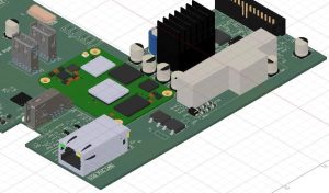
PCB design by Devtank
DFT overview
The situation for DFT can often be very different and DFT aspects are often only considered just prior to a production run, particularly if the design authority is relatively new to producing and testing PCBAs. The following overview is aimed to help capture the majority of points to consider relating to DFT. If the PCBA design is dense and complex some of the wish-list requirements may not be implementable or deemed too time consuming to implement or potentially could lead to the requirement for further prototyping and design verification phases. In an ideal world DFT will get more consideration earlier on in the design process but this generally comes with more experience.
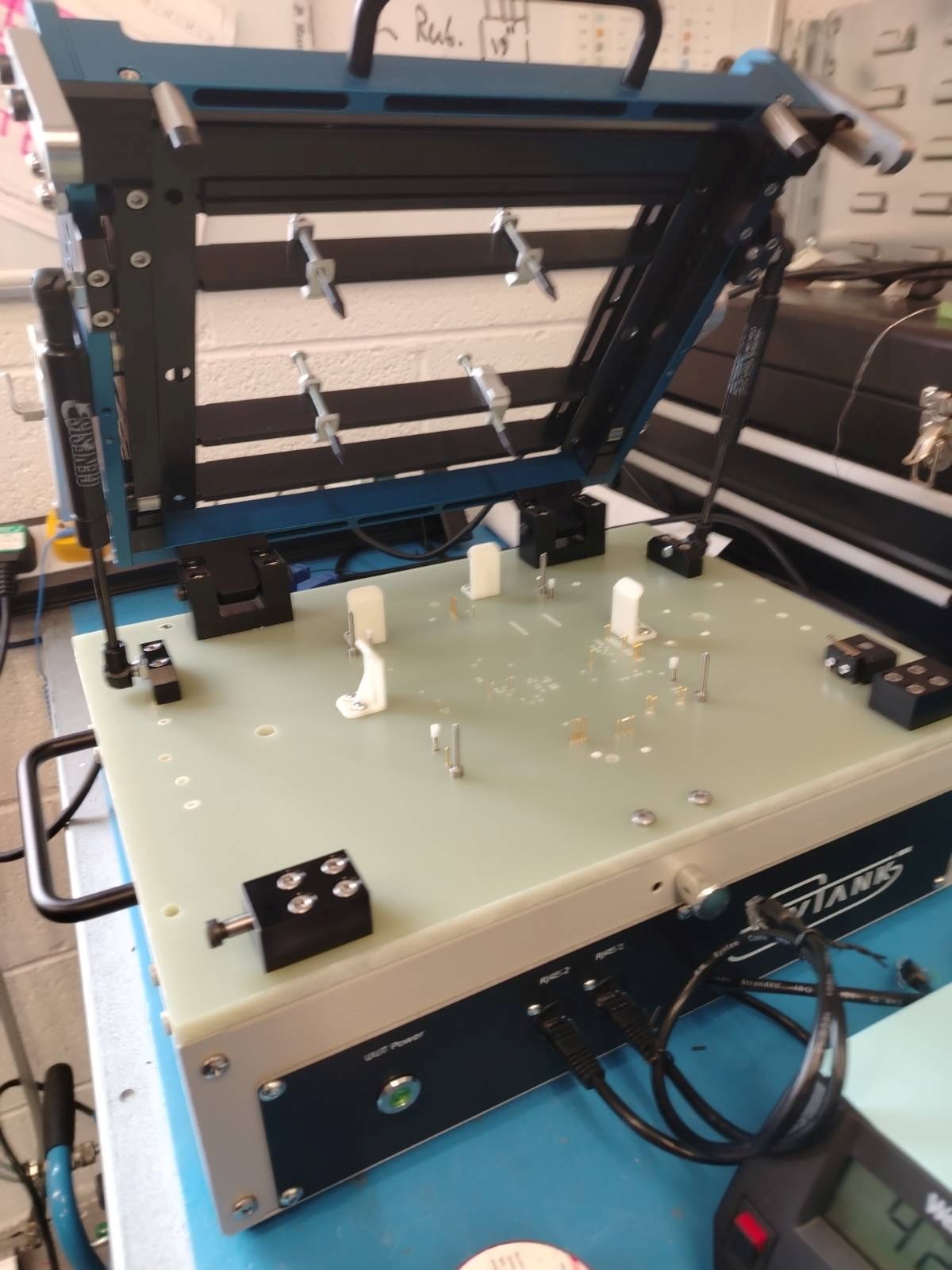
The basic requirement for the PCBA is to have Test-points (TPs) that a test-fixture can either monitor or drive test signals. The number of test-points in a design will vary based on the design complexity. Generally speaking we would recommend adding a good amount of test-points into a design from the outset. A decision can be made further down the design road as to whether DFT Hardware (Test Fixture) will use these TPs or not. Test points are the first discussion point we’ve provided.
DFT requirement: Test point quantity
Detail design considerations: Add-in Test-points to the Schematic/PCB Designs for all:
- Power Supply Lines
- Key/Critical signals to be monitored
- Through hole pins requiring probing rather than using the connector lead or pin.
This applies to both connectors (where possible) and all conventional leaded components.
Ideally full-coverage of all test nodes should be covered with unique test-points i.e. no probing of any through hole leads unless unavoidable or not practical because of the quantity.
Note: The main benefits for the approach detailed in point C are:
(i) The target areas for the test-pins will be clean and flux free.
(ii) The test fixture can be designed using the least amount of test pin types making servicing easier and removing cost.
DFT requirement: Test points location
Detail design considerations: Decide which side of the PCBA to place the test-points – ease of connectivity may be a deciding factor. Unless unavoidable, all test-points should be on just one side only of the PCBA. (Sometimes this just isn’t possible but in that instance the designer should aim to have a side nominated for the bulk of the test pads to simplify the test fixture design.
DFT requirement: Test points type and geometry
Detail design considerations: Test-point geometry should be a plain circular pad with no-drill and solder mask removed. Finish – Preferred finish ENIG. Test-point pad minimum diameter of 1.50mm, generally larger test pads provides a more forgiving landing area but needs managing carefully to not degrade signals, e.g. high speed communication.
DFT requirement: Test point spacing
Detail design considerations: Minimum spacing (default) of 2.54mm (On dense designs this may need to be reduced to 2.00mm or 1.27mm).
DFT requirement: Test points board detects
Detail design considerations: The design should incorporate test-points ideally in each corner of the PCBA. These should be the standard geometry test-pads and they should be connected to the ‘GND’ or ‘0V’ net of the design.
Note: These are used as feedback test-points to indicate that the PCBA under test is located correctly on the fixture. i.e. all 4 nodes should feedback a ‘GND’ or ‘0V’ connection. If it is difficult to implement 4 ‘DETECT’ test-points then a minimum of 2 diagonally orientated should be used.
DFT requirement: PCB design – tooling holes
Detail design considerations: For the test fixture to register the PCBA to the test pins there should be a minimum of 2 tooling holes (ideally 3 or 4) added to the design. For larger boards, >250 mm square say > 4 tooling holes recommended. These should be non-plated holes where possible.
Note: If the design already includes a number of FIXING holes, e.g. used to mount in an enclosure, these can be used also for tooling purposes and avoid the need to add further holes.
DFT requirement: In-circuit Programming
Detail design considerations: Many boards will contain micro-controllers or processors which need programming as part of the production process. It’s relatively easy to incorporate this in the test sequence if access to programming pins is provided by adding test pads for your standard programming interface, e.g. Serial UART, SWD/SWCLK, I2C bus and JTAG. These connections also enable debugging and interrogating of the software during the test process to validate the correct functionality.
DFT requirement: Panellisation
Detail design considerations: The CM may produce the PCBA in panels of 2/4/ or > depending on the size of the assembly. Prior to test the substrates should be removed from panellisation prior to test.
Note: It is not recommended to test the substrates whilst in panelled format.
This approach would mean undesired breaking out/routing processes to take place on tested assemblies. This introduces several risks to the passed PCBA from both the mechanical stress, potential dust and debris contamination plus the additional ESD risk from more handling processes. Also, if the CM is changed the new CM would be required to produce a panel that met the original design exactly, accuracy of step and repeat, tooling features etc. Something that they may or may not not be able to agree to.
DFT requirement: PCBA Voids
Detail design considerations: Ideally there should be 3 or 4 areas within the PCB design where there are no SMT parts or tracking. These areas can be utilised for mechanical push rods, used to push the PCBA down onto the test pins, once clamped inside a test fixture.
It is best to push on blank pcb areas rather than using bulky components, e.g. large connector or relay, but sometimes the latter may be unavoidable.
DFT requirement: PCB Material Thickness
Detail design considerations: Generally standard FR4 1.60mm is appropriate for small to medium size PCBAs.
If the PCB dimensions are large, say > 250mm square and there are a large number of test points required, the force required to push the PCBA down on the fixture can be large. This can cause the PCBA to bend/flex. This can cause SMT joint cracking to occur.
To mitigate this risk, have the PCB manufactured in 2.0mm or 2.40mm material.
DFT requirement: Labelling – QR or bar code
Detail design considerations: It is recommended that a labelling system is put in place for all assemblies to be tested. This may require an area of the PCB to be set aside for a label, e.g. barcode or QR code type that can be read with a barcode/QR code scanner. This is very advantageous for assembly tracking and logging of test results that can be saved in a database.
What is Design for Manufacture (DFM)?
Design for Manufacture (or Design for Manufacturability) is the process of designing a product with the manufacturing process in mind, so that the product can be produced more easily, reliably, quickly and at lower cost.
In electronics and PCB manufacturing specifically, that means asking questions early in design such as:
- Are component footprints optimised for standard pick-and-place and reflow processes?
- Is the PCB layout compatible with the fabrication house’s capabilities (minimum trace widths, via sizes, panellisation, solder mask clearances)?
- Have we minimised unnecessary complexity in assembly (number of parts, mechanical assembly steps, custom fixings)?
- Is the supply chain stable (part availability, alternative sources, common components)?
According to industry guidance, up to 70% of manufacturing cost can be locked-in by design decisions made at the early stage. That means if you shift those decisions left, into the design phase, you gain huge leverage.
What is Design for Test (DFT)?
Design for Testability is about designing your product so that testing (during production and afterwards) is efficient, effective and reliable. In other words: making sure that you can actually prove your boards, modules or systems are working, and catch defects early and completely.
In practical PCB / electronics manufacturing that looks like:
- Including dedicated test‐points, probe pads, boundary scan or built-in-self-test features.
- Designing for access (mechanical and logical) so that automated test equipment (ATE) or fixtures can connect reliably.
- Ensuring that test coverage is high (you are not shipping products you haven’t adequately tested), reducing life-field defects and returns.
- Embedding traceability, data capture and test logs (something we emphasise at Devtank in our production test platforms).
Why DFT and DFM matters for Devtank clients and the manufacturing ecosystem
Here at Devtank Ltd (with our background in PCB manufacturing test-solutions, custom fixtures and production test platforms such as HILTOP) we see the advantages of applying DFM and DFT early in multiple ways:
- Faster time to market – by avoiding repeated redesigns, manufacturing fix-ups and test fixture re-work.
- Higher yields and fewer defects – good DFM reduces scrap, rework and hidden costs; good DFT catches faults early and ensures quality.
- Lower total cost – not just BOM cost but manufacturing cost, assembly cost, test-cost, warranty/return cost.
- Better scalability – when you design with manufacturability and testability in mind you are set up for volume production rather than just small runs.
- Traceability and process control – good test design means better data, better insight, and tighter process control (something our HILTOP platforms deliver).
For instance, in our PCB test solutions page (visit here) we emphasise that automated, repeatable, accurate testing contributes to improved quality, reduced waste and lower costs.
Make DFM and DFT standard practice
Due to our expertise and service offering, we always make Design for Manufacture and Design for Testing standard practice.
In our opinion designing a great product is no longer enough. For electronics manufacturers, the real competitive edge comes when that product is designed to manufacture easily, test reliably, assemble efficiently, and scale robustly.
For clients of Devtank, whether you’re doing one off prototypes or moving into volume production of PCBAs, modules or systems, invest early in DFM and DFT. It pays dividends in reduced cost, improved quality and faster time-to-market. Trust us, we’ve seen that in evidence over the years!
If you’d like to explore how Devtank can help you integrate manufacturability and testability into your next project, especially with our modular platforms, custom test fixtures and end-to-end production test solutions, please get in touch.